
ALD for electronic devices
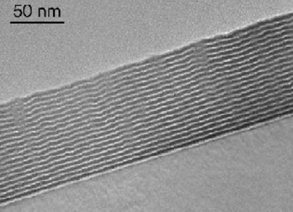
Atomic Layer Deposition (ALD) is a thin film deposition technology and a special kind of Chemical Vapor Deposition (CVD). The thin film growth by ALD takes place in individual cycles and usually under vacuum. Each cycle deposits a well-defined layer thickness, ideally one atomic monolayer. One cycle usually consists of four individual temporally separated steps (i. adsorption of precursor 1; ii. purging; iii. adsorption of precursor 2 and reaction with adsorbed precursor 1; iv. purging). Since each precursor cannot react with itself no further reaction takes place after a complete saturation of the surface. Therefore, the film growth is self-limited and complex two- and three-dimensional structures can be precisely coated with conformal thin films.
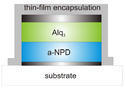
At the Chair of Electronic Devices ALD on the one hand is used as a powerful and precise thin film deposition technology for the development of new electronic and optoelectronic devices. On the other hand we carry out research on ALD itself and we develop new ALD processes like plasma ALD, spatial ALD and atmospheric pressure ALD.
ALD for electronic devices
ALD research
Latest posts
More information about #UniWuppertal: