
Analytics for failure analysis and reliability investigations
Failure analysis and reliability investigations at the chair of Electronic Devices are done by development and optimization of scanning probe (Scanning Near-field Optical Microscopy and Scanning Force Microscopy) and scanning electron microscopical techniques as well as their combination to hybrid systems. The focus in research is on the detection and correlation electronic, opto-electronic, thermal, and micro-mechanical properties of starting materials as well as fabricated devices.
Scanning Electron Microscopy
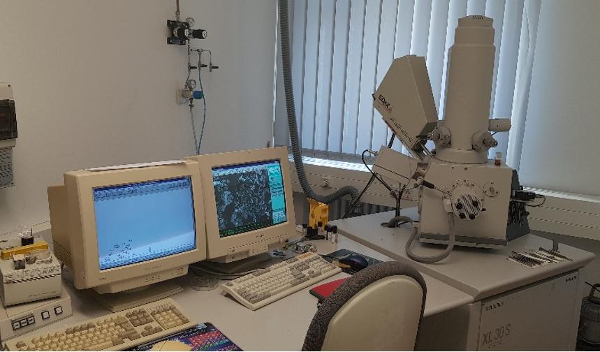
High-resolution inspections of the morphological and chemical analysis by means of x-ray fluorescence microcopy (EDX) on materials and devices are carried out. Vacuum unfriendly, vacuum intolerant, as well as samples with low electrical conductivity are inspected by an Enviromental Scanning Electron Microscope (ESEM).
Electrical field distributions within a device can be detected for instance by beam induced currents even on active devices. Variation of electrical field strengths during a switching event of a power diode are obtainable.
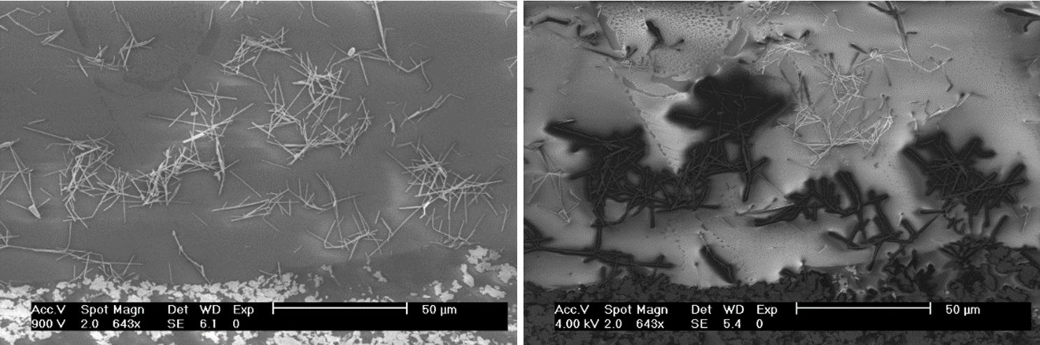
Failure localization is carried out by means of active and passive voltage contrast. In case of Ag-nanowires on glass, the charging of the insulating glass substrate can be avoided at 900 V acceleration voltage, as the charge (introduced to the sample by the electron beam bombardment) is balanced by the charge that leaves the sample as secondary or backscattered electrons. For higher acceleration energies (4 keV), charging of the sample takes place in the open area of the AgNW mesh resulting in an electron beam induced potential. contrast.The regions close to the conductive and grounded AgNW on glass appear dark, as the excessive charge is transferred to the ground.
Scanning Probe Microscopy
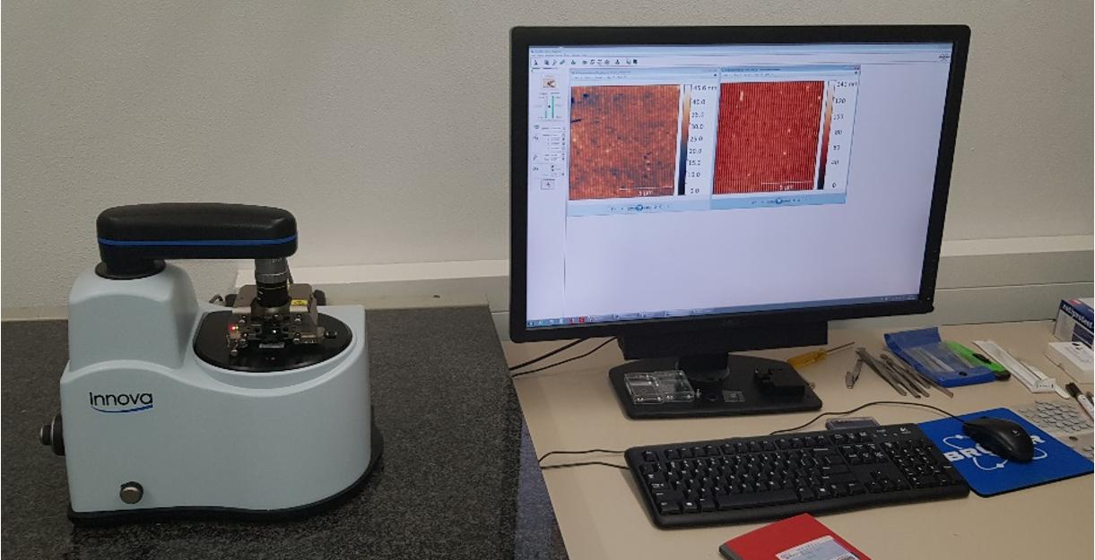
The topography of our samples is detected by contact, non-contact, and tapping mode AFM. Local variations in work functions or differences in potentials can be characterized with highest resolution either by Kelvin probe force microscopy or electric force microscopy.
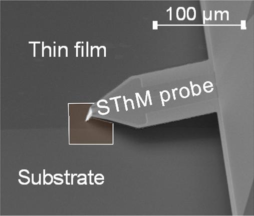
Cross-plane and in-plane thermal transport in ultrathin films can be studied successfully with Scanning Thermal Microscopy (SThM). Heat transport characteristics, that were previously accessible only by simulations, e.g. the Stefan-Boltzmann transport equation, were evidenced experimentally for the first time. Ballistic transport mechanisms have been demonstrated at film thicknesses significantly larger than the mean free phonon path lengths, which is in contradiction to the usual macroscopic diffusive description.
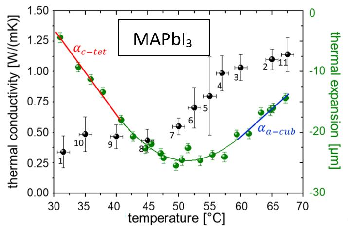
Thermal conductivity measurements on organic−inorganic hybrid perovskite thin films is of paramount importance for optimal performance and reliability. The thermal conductivity of all-inorganic as well as on hybrid halide perovskite single crystals and thin films is analyzed by SThM. The temperature dependence of the thermal conductivities and of thermal expansion coefficients are detectable.
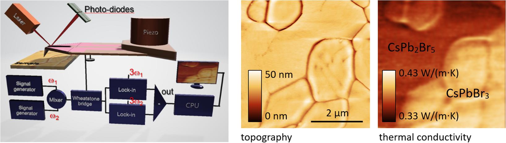
In order to determine the low thermal conductivity in perovskite thin films with high spatial resolution using the 3Ω-technique, we employ a thermal conductivity mapping in the frequency domain. Local thermal conductivity, thermal diffusivity, and volumetric heat capacity are mapped simultaneously.
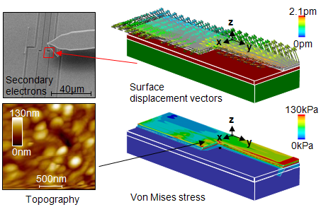
The detection of periodic deformations can be detected with very high sensitivity and thermal elastic properties can be obtained by correlation and attributed to basic physical principles. Thermally induced strain and stress on a constriction of an interconnect structure can be detected for instance.
Hybrid Systems
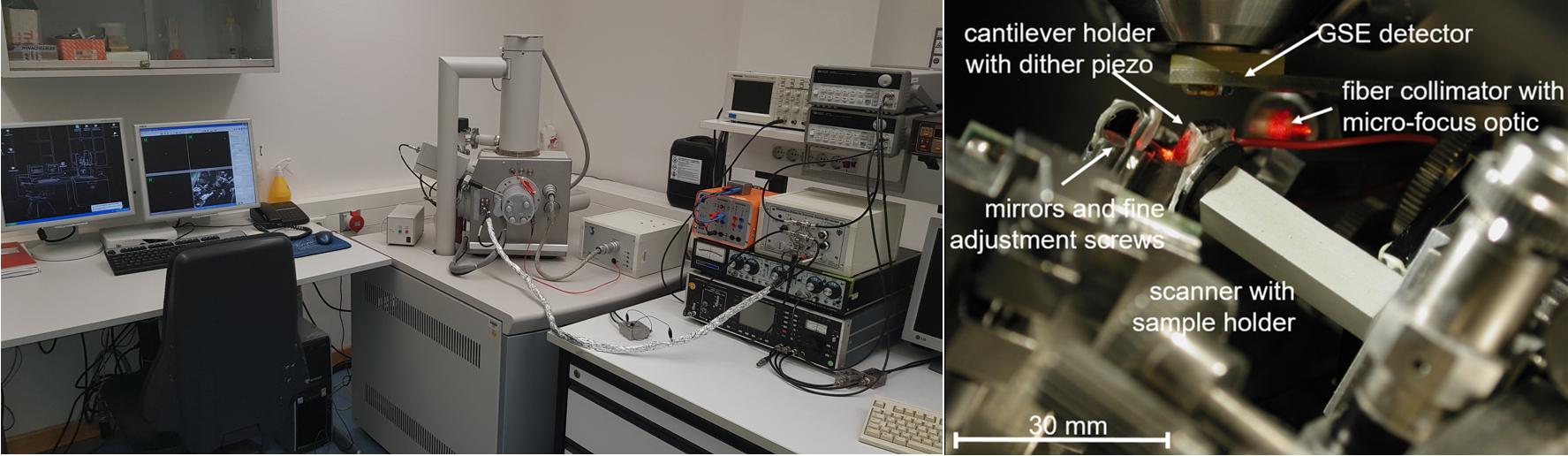
Scanning Probe Microscope is integrated into the analysis chamber of an ESEM. Promising for future applications is the fact that the used probes can either be used as sensors, which give access to a vast variety of material properties, or as actuators, which can deliberately modify samples at a level of a few millionth millimeters (nanometer).
Publications
Gomella L., Haeger T., Roscher M., Bishara H., Heiderhoff R., Riedl T., Scheu C., Gault B.: “Microstructure manipulation by laser-surface remelting of a full-Heusler compound to enhance thermoelectric properties” Acta Materialia 223, (2022), 117501, DOI: 10.1016/j.actamat.2021.117501
Haeger T., Heiderhoff R., and Riedl T.: “Thermal properties of metal-halide perovskites“ Invited Review J. Mater. Chem. C, 2020, 8, 14289 - 14311 DOI: 10.1039/D0TC03754K
Haeger T., Ketterer M., Bahr J., Pourdavoud N., Runkel M., Heiderhoff R., and Riedl T.:"Thermal properties of CsPbCl3 thin films across phase transitions“ (2020) J. Phys. Mater., DOI: 10.1088/2515-7639/ab749d
Haeger T., Wilmes M., Heiderhoff R., and Riedl T: “Simultaneous Mapping of Thermal Conductivity, Thermal Diffusivity, and Volumetric Heat Capacity of Halide Perovskite Thin Films: A Novel Nanoscopic Thermal Measurement Technique”, J. Phys. Chem. Lett. (2019), 10, 3019−3023, DOI: 10.1021/acs.jpclett.9b01053
Heiderhoff R., Haeger T., Pourdavoud N., Hu T., Al-Khafaji M., Mayer A., Chen Y., Scheer H.-C., Riedl T.:"Thermal Conductivity of Methylammonium Lead Halide Perovskite Single Crystals and Thin Films – A Comparative Study" The Journal of Physical Chemistry C (2017), DOI: 10.1021/acs.jpcc.7b11495
Heiderhoff R., Haeger T., Dawada K., and Riedl T.: “From diffusive in-plane to ballistic out-of-plane heat transport in thin non-crystalline films” presented at ESREF 2017, 28th European Symposium on Reliability of Electron Devices, Failure Physics and Analysis, September 25th -28th, Bordeaux, France, (2017), Microelectronics Reliability,76-77 (2017), 222-226, DOI: 10.1016/j.microrel.2017.06.064
Buege M., Koehler T., Heiderhoff R., Papenheim M., Wang S., Schleiting H., Arnold W., Foerst J.R., Seyfarth M., Tiroch K., Riedl T., and Vorpahl M.: “Minor defects of the luminal integrity in arterial introducer eSheaths after transcatheter aortic valve implantation" PLOS ONE (2017), DOI:10.1371/journal.pone.0176893
Makris A., Haeger T., Heiderhoff R., and Riedl T.: “From diffusive to ballistic Stefan-Boltzmann heat transport in thin non-crystalline films” RSC Advances (2016), 6, 94193-94199, DOI: 10.1039/c6ra20407d
Heiderhoff R., Makris A., and Riedl T.: “Thermal microscopy of electronic materials” Invited Paper Materials Science in Semiconductor Processing, Volume 43, (2016) 163–176 doi:10.1016/j.mssp.2015.12.014
Heiderhoff R., Li H., and Riedl T.: “Dynamic Near-Field Scanning Thermal Microscopy on thin films” presented at ESREF 2013, 24th European Symposium on Reliability of Electron Devices, Failure Physics and Analysis, September 30th - October 4th, Arcachon, France, (2013), Microelectronics Reliability, Vol. 53, Iss. 9–11, September–November (2013), 1413–1417
Zilberberg K., Gasse F., Pagui R., Polywka A., Görrn P., Behrendt A., Trost S., Heiderhoff R., and Riedl T.: “Highly robust Indium-free transparent conductive electrodes based on composites of silver nanowires and conductive metal oxides”; Advanced Functional Materials (2013), DOI: 10.1002/adfm.201303108, 8 pp
Heiderhoff R.; “Advanced SEM/SPM microscopy”; Invited Paper presented at IPFA 2012, The 19th International Symposium on the Physical and Failure Analysis of Integrated Circuits, Marina Bay Sands, Singapore, 02-06 July, (2012), IEEE 978-1-4673-0980-6 (2012), DOI: 10.1109/IPFA.2012.6306335, 4 pp
Heiderhoff R. and Balk L.J.; “Scanning Probe Microscopy-History, Background, and State of the Art”; in Handbook of Nanoscopy (Wiley-VCH, Weinheim, Germany, ISBN: 978-3-527-31706-6); edited by Gustaaf Van Tendeloo, Dirk Van Dyck, and Stephen J, Pennycook; Volume 1; Chapter 15; (2012) 499- 538
Fakhri M., Geinzer A.-K., Heiderhoff R., and Balk L.J., “Nanoscale Thermally Induced Strain and Stress Analysis by Complementary Scanning Thermal Microscopy Techniques“, Invited Paper presented at the 18th International Symposium on the Physical and Failure Analysis of Integrated Circuits, Incheon, Korea (South), Jul 4 - 7, (2011), Proceedings of 18th IPFA, IEEE 978-1-4577-0158-0/11/$26.00 (2011) 18
If you have any queries please do not hesitate to contact
Dr.-Ing. Ralf Heiderhoff
Bergische Universität Wuppertal Fachbereich Elektrotechnik, Informationstechnik, Medientechnik Lehrstuhl für Elektronische Bauelemente Rainer-Gruenter-Strasse 21 D-42119 Wuppertal Gebäude: FG / Raum: 1.14
Tel: +49-(0)202-439-1966 Fax: +49-(0)202-439-1412 E-mail: heiderho[at]uni-wuppertal.de